Friday, November 30, 2012

Visit Canon Opto Malaysia


Hello guys! This week I and my friend go to visit Canon Opto Malaysia. So, I would like to tell a story during the visit. The visit is on 27 Nov 2012 and whole SMJE first year student compulsory to join the visit. The lecturer that join the visit is Mr Redzuan and Dr Muzahidul Islam. We start our journey at 8am and finish at 12.30pm. 

Shortly after arriving in canon opto, we are welcome by 3 of their workers. Then, we take a picture whole group by Canon staff. After that, we go to hall for briefing by Canon staff regarding program flow. We are so excited have a chances to visit Canon Opto. Canon Opto is famous with camera and lens product. Firstly, we are going to visit waste management area. There we can see many chemical being process and separate to reduce the toxic. At the same time, the engineer told us about Canon Opto policy. Their policy is " To reduce adverse impacts of the company operation towards protection of environment by necessary mean and actions for a better and harmonious environment".

After visit the waste management site, we going back to hall to get another briefing from person in charge. Now, we going to visit manufacturing site. There we cannot take any picture or video due to company rules. We only can see the process only. In manufacturing site we can see the process assemble of camera and lens. Mostly the operator is woman and beautiful. The do the job very careful and nice. The process a bit complicated because they need to do properly.

Below is the picture with the Manager for waste management.


Picture below is the water treatment machine.


Lastly before we going back, Canon Opto give us a souvenir to us. We are glad to get the souvenir. Canon Opto also provide us with lunch before we are going back to campus.

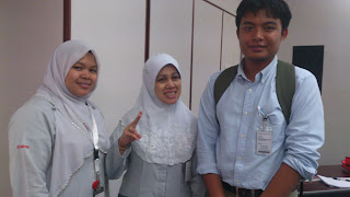
Before going back, I also snap a picture with a Canon Opto Corporate Communication staff.


Thank you MJIIT and Canon for this visit..

Thursday, November 22, 2012

Electronic Systems in Industry


Hello guys! This week we will talk about electronic systems in industry. For this week, MJIIT invite Mr Vivek Panicker from Titan Thermal Solutions. Mr Vivek have wide experience in this industry.Especially in thermal imaging.

This week we are glad that we have chances to get the info from Mr Vivek. In his slide, he divide the topic into 4 branch. There is electronic systems, role of electronic systems, imaging industry and electronic with thermal imaging. Nowadays, electronic systems is widely use in all area.Especially in manufacturing industry. Electronic systems is used to replace previous system and make it more reliable. In future, all the system will become more complex but easily to be use. 

Below is the picture from Mr Vivek presentation. He describe the definition of electronics.

                               Definition of electronics

Below is the flow of electronic systems from the early introduction until now. From large PCB to the miniature. From simple system to complex architecture and from analog to digital. All this changes give benefit to use especially to end user and industry.

                                Flow of electronics

Next topic is the role of electronics in industry. Nowadays many company depends on electronics in their industry. Here also I put a picture focus on the role of electronics in industry.

                               Role of Electronics in Industry

For your information, role of electronics in industry classified into consumer electronics, industrial electronics,  defense and communications. This four sector is very important in global industry.

                              Sector in electronics industry

Now Mr Vivek explain more detail regarding imaging industry. For me, this topic still new because a bit complex to understand. There are 8 type of imaging we have globally. There are chemical imaging, digital imaging, geophysical imaging, medical imaging, molecular imaging, optical imaging, radar imaging and thermography.

                                      Imaging Industry


In his presentation he explain about pixel and resolution. A digital image is formed by pixel. There a smallest information in an image.Pixel often represented using dots, squares or rectangle. More pixel and resolution more sharp the image.This technology is use by camera. Mr Vivek also told us that digital stream video is made of a group of pictures (frames) captured across a period of time. This info is very important for us as engineering student. Mr Vivek also explain about the format of video. NTSC is for analog television and PAL for analogue television color encoding system used in broadcast television systems. This format also support all new TV (LED,LCD and Plasma)

National Television System Committee (NTSC) & Phase Alternating Line (PAL)

  • Human eye requires a minimum 25 frames per second.
PAL TV standard
  • 25 frames per second (25 hertz or 50 hertz half frame)
  • Resolution of 320 by 720.
  • Asia, Europe, South America and East Africa.
NTSC TV standard
  • 30 frames per second (30 hertz or 60 hertz half frame)
  • Resolution of 480 by 720.
  • North America and Japan.
Lastly Mr Vivek explain about electronics within thermal imaging industry. Thermal imaging a spin off defense electronics. It make use of wavelengths in 7-14 μm to form an image. Thermal requires non-uniformity calibration (NUC) on data stream. Data varies in state and space. Its also enables implementation of intensive algorithms such as Kalman filters, edge detection, neural network modelling.

Below is the equation for incident energy.

Incident Energy (I) = Emitted Energy (E) + Transmitted Energy (T) + Reflected Energy (R)

I is the energy profile when viewed through a thermal imaging camera. E is generally what is intended to be measured. T is the energy that passes through the subject from a remote thermal source. R  is the amount of energy that reflects off the surface of the objects from a remote thermal source.


Friday, November 9, 2012

Japanese Work Culture


Hello guys, This week we have one invited presenter from Canon Opto Malaysia. He is Mr Muhammad Azlan Bin Amran. He is Senior General Manager , Administrator Centre at Canon Opto (M) Sdn Bhd in Shah Alam.

During his presentation, he introduce about Canon. Canon Opto (Malaysia) Sdn Bhd was incorporated in 1988 as part of global growth of the Canon group based on Canon's corporate philosophy of world prosperity and human happiness. Canon Opto is located in Shah Alam, Selangor with a land area 131,600 square meters and paid up capital RM 113.4 million.

Below is one picture taken during the presentation.


In this presentation also, Mr Azlan introduce to us  manufacturing company roles in product life cycle.
Below is some picture taken during the presentation.


The above picture, Mr Azlan explain that engineer must transform a prototype product into a mass production product. This process very important before produce the product.


Above picture show the process to make the lens. There are many process to be follow before complete the product.


In the upper picture, there are combination of optical, mechanical and electronic before assemble the complete lens.


In above picture, to assemble the lens they have to combine the components and then do an adjustment and lastly do an inspection.

Now, Mr Azlan introduce to us the Japanese work culture concept. There are many concept to be follow and practice.The first concept is Horenso. In Horenso there are three component inside the Horenso. There are Houkoku, Renraku and soudan. Below is the picture from the presentation slide.

                                     HORENSO


In above picture doing a report is very important skill in working environment. This make our work more structured and systematic.


To make a report in working environment, we should always start form conclusion. Working report is totally different with our school report. Once we start our working, we should practice this.


In upper picture, if we found any accident in working environment we should contact the superior to inform the incident in detail.


Next Japanese working culture is San-gen. San-Gen is important to all staff to practice. Especially in factory environment. Below is the picture.


Lastly in this presentation is 5S. Many company apply this concept include government agencies. Below is the poster.


That all for this week. I hope you all can apply this Japanese working culture anywhere in your life. This will change your lifestyle to become more systematic. See you all next time with other topic.

Friday, November 2, 2012

Introduction to Bioelectronics

Hello guys!! How are you? Hope you all happy with your life. On 30th October 2012, Dr Azran Azhim give a lecture about the Introduction to Bioelectronics. This is the first time we meet him. In his presentation he focus more about electronic in biology sector. In Malaysia, this sector still new for us compared to other country like Japan, USA and other.

To create more professional engineer in bioelectronics sector, we should study and do more research regarding application of electronic in biology.  Definition about Bioelectronics in Dr Azran Azhim presentation is a recently coined term for a field of research that works to establish a synergy between electronics and biology. In his presentation also he introduce us with a few picture of circuit.
There are series and parallel circuit. Below is the picture of circuit from Dr Azran Azhim slide show.

                                          Series and Parallel Circuit

Dr Azran Azhim also explain to us about RC circuit and CR circuit. This two circuit have different function. RC circuit act as a low pass filter circuit. While CR circuit act as a high pass filter circuit. Below is the picture  for both RC and CR circuit.

                                          RC circuit

                                          CR circuit

In this presentation, we learn many new circuit. But not in detail because this just a short lecture. At the same time, Dr Azran Azhim introduce to us about Active electronic realization. In this topic, have 2 type of first order active low pass filter and first order high pass filter. Here also he gave us Estimation method chart.Below is all the picture from the presentation slide.

                                          Active electronic realization

                                          Estimation Method

Here also we know about the doppler probe and effect. Doppler probe is device used in medical applications to measure shift sound waves emitted by and bounced back to device. This probe allows measurement and either visualization or audio simulation of the movement of substances within body. This doppler probe are most often use in cardiovascular application and monitoring pregnancy.

Doppler effect is the change in frequency of a wave, usually in sound wave. Each frequency appears higher when an object getting closer to observer and lower when its moving away.

Last but not least, Dr Azran Azhim told us about Shinya Yamanaka. Shinya Yamanaka wins 2012 Nobel Prize in medicine. Shinya Yamaka is a senior investigator at the Gladstone Institutes is also a professor at Kyoto University.

Therefore, Bioelectronics is an interesting field. For those who wish to majoring in this field, they have to work hard to excel in competitive environment. Nothing is impossible to success in this field. With the prayer and constant study is the most important to achieve this mission.
See you next time.